
La/Sr diffusion
La/Sr diffusion
In thin film growth, we usually assume that a chemically homogeneous crystal phase forms. This assumption is generally true when films are grown at high temperatures and the surface atom mobility is high. On the other hand, when preparing heterostructures, we would like to see atomically sharp interfaces with minimal interdiffusion. Obviously, it can be difficult to achieve both goals simultaneously, especially when working with perovskite materials that can easily accommodate dopants over a wide composition range.
It is therefore important to evaluate the diffusivity of component cations in materials that meet at a heterostructure interface. This experiment illustrates a case where a LaFeO3 film is grown on a SrTiO3 substrate and the diffusivity of Sr in the film is evaluated by measuring the Sr content on the LaFeO3 film surface. Ideally, of course, there should be no Sr on the film surface. However, both LaFeO3 and SrTiO3 have a similar perovskite structure, and either La or Sr can occupy the perovskite A-site position.
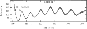
Fig. 1: RHEED specular spot intensity oscillations during LaFeO3 growth.
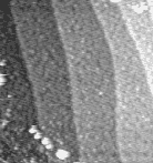
Fig. 2: STM image of a LaFeO3 film surface after deposition at 600°C on a 0.05% Nb:SrTiO3 substrate. 400 × 400 nm2
A thin LaFeO3 film was grown on a step-and-terrace SrTiO3 substrate at about 600°C. At this temperature, the film grows in a layer-by-layer mode and we can determine the film thickness by counting the RHEED specular intensity oscillation. As shown in Fig. 1, the film thickness was about 7 monolayers (~3 nm). An STM image of the surface (Fig. 2) still shows a clear step structure. Some roughness is visible on the terraces, as expected for layer-by-layer growth. Bulk diffusion should be very slow at 600°C, which means that we would expect negligible long-range diffusion to occur, but as indicated by the surface roughness, the film is likely to contain many random pint defects.
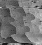
Fig. 3: STM image after annealing. 400 × 400 nm2
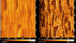
Fig. 4: AFM and FFM images of the annealed surface. 1000 × 1000 nm2
The point defect density in a film can be reduced by increasing the growth or annealing temperature. This allows atoms to migrate in the crystal and the total crystal energy can be minimized by ejecting defects, assuming that the average stoichiometry is correct. While annealing generally improves the crystallinity of a film, it may also lead to additional interdiffusion at an interface.
The LaFeO3 film was annealed at 1000°C for 15 minutes at 10-4 Torr oxygen. STM (Fig. 3) showed a dramatic change in the surface morphology, with considerably smoother terraces and meandering step edges. STM is not particularly sensitive to surface termination changes. The film was therefore removed from the chamber and AFM/FFM images were taken in air. The advantage of friction force microscopy (FFM) is that it can detect macroscopic regions with different chemical composition on a flat crystal surface. In this case, the simultaneously acquired AFM and FFM images in Fig. 4 show that there are definite contrast differences on otherwise flat terraces. The darker patches in the FFM images are presumably due to segregated Sr on the film surface.
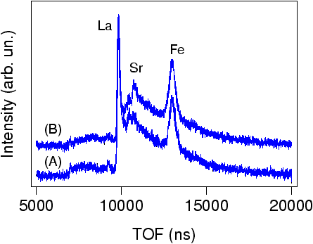
Fig. 5: CAICISS time of flight data before (A) and after (B) annealing the film
The chemical changes on the LaFeO3 film surface were analyzed by CAICISS by measuring the ion scattering spectra before and after the annealing treatment. As shown in Fig. 5, there are strong La and Fe scattering peaks, but no Sr signal in the time-of-flight spectrum (A). A clear Sr peak appears during annealing as shown by spectrum (B). This confirms that the contrast seen in FFM images is indeed related to the appearance of Sr on the film surface. The experiment shows that Sr from the substrate migrated through a 3 nm film in just 15 minutes at 1000°C. Such fast interdiffusion doesn't always occur. This is a special case for structurally matched materials like LaFeO3 and SrTiO3.