Oxide thin films
Transition metal oxide thin films are widely used for basic materials
science and in various device applications.
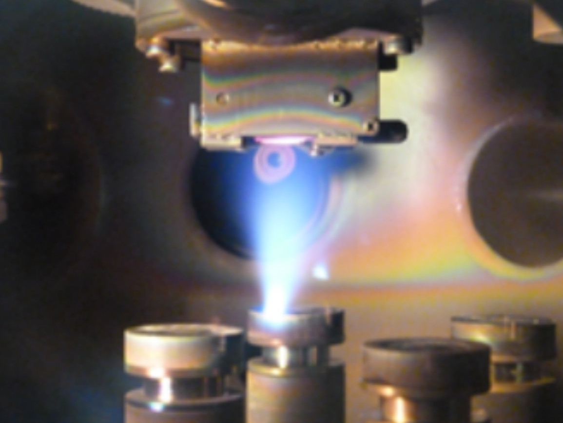
We study the properties of oxides in confined
geometries, typically in the form of thin films grown by
Pulsed Laser Deposition (PLD). PLD gives us the flexibility to work
with very many different oxide materials and to combine different
oxides in heterostructures. With the help of in-situ electron diffraction (RHEED),
oxide thin films can be grown with single atomic layer accuracy.
The pulsed deposition regime can be used to control the kinetics of crystal growth.
This is particularly useful in the growth of nanostructures.
Since films are grown on single crystal substrates, it is often possible to choose
the crystal orientation and the epitaxial strain state in a film.
You can read more here about the design and construction of the
PLD chambers that we use in our research.
Oxide photocatalysts
Solar-powered splitting of water into hydrogen and oxygen on
the surface of an oxide semiconductor photocatalyst carries the promise
of clean hydrogen fuel production. A new class of optical-quality
oxides is required for this technology to become competitive with
other solar energy capture techniques. Our purpose is to study
doping mechanisms of well-known wide-gap oxides to develop an oxide
semiconductor that is stable in water, has an optimal band gap for
absorbing sunlight and splitting water, and sufficiently low trapping and
recombination losses for high energy conversion efficiency.
Surfaces
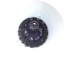
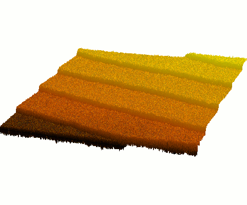
Thin films are usually grown on single-crystal substrates and the crystallinity
of the film is strongly affected by the morphology and stoichiometry of the
substrate surface. It is therefore desirable to start film growth
with an atomically flat surface that has a well-defined miscut angle
and direction. Preparation of such 'step-and-terrace' surfaces requires
a combination of polishing, annealing, and chemical etching treatments. The
surface morphology can be characterized by atomic force microscopy and in-situ
electron diffraction. The composition of the surface can be determined by
ion scattering spectroscopy. Read more on surface dynamics and SrTiO3
surface preparation:
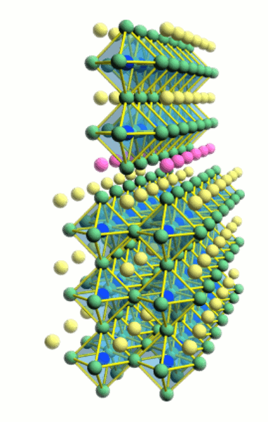
Interfaces
The properties of materials are different close to a surface
or an interface. In the simplest cases, the properties change due to
carrier density profiles caused by band bending, but more complex cases
are possible as well. The most interesting cases are those where completely
new phases appear at interfaces, such as metallic conductivity in an insulator
or magnetic order in a nonmagnetic host material.
Due to the layer-by-layer growth of thin films, it is possible to fabricate
atomically sharp interfaces and delta-doping layers. However, since oxide films
are grown at high temperature, it is always questionable whether the interfaces
are truly atomically sharp and no interdiffusion has occurred. Ion scattering
spectroscopy is a useful tool for analyzing interdiffusion in ultrathin oxide
films. Read more about film composition analysis and diffusion measurement:
Nanostructures
Combined thermodynamic and kinetic crystal growth control can be used to
grow a variety of oxide nanostructures. Fast growth at low temperatures nucleates
nanodots that can be grown into larger nanostructures, such as pyramids or pillars,
or annealed to form percolative nanostructure arrays. Slow growth at high temperature
can be used to fabricate nanowires on step-and-terrace crystal surfaces. As long as
the nanostructure growth remains epitaxial, cation interdiffusion is minimal and
even single unit cell nanostructures are stable. Read more about the materials and types
of oxide nanostructures that can be grown by pulsed laser deposition:
