This year we can accept up to two M1 students.
If you wish to enter the doctoral course, please contact us.
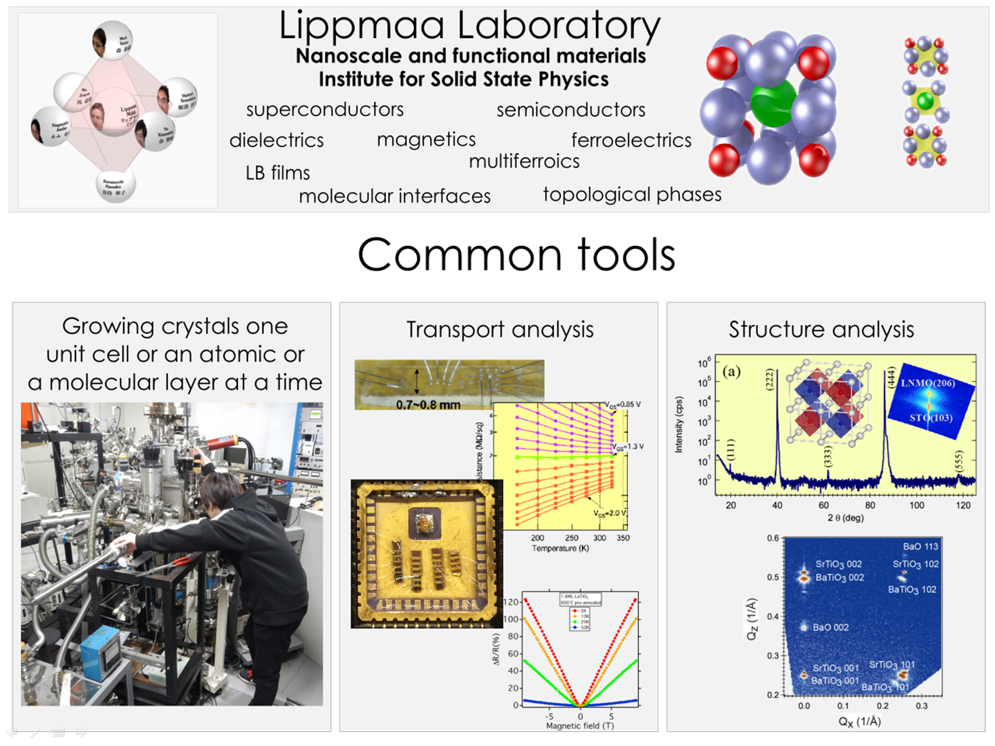
All projects in this laboratory involve thin films of
transition metal oxides. There are many interesting oxides, such as
high-temperature superconductors, photocatalysts, magnetic materials,
ferroelectrics, multiferroics, semiconductors, wide-gap dieectrics, etc.
We study many different materials, but usually in the form of very thin layers,
in heterostructures or in the form of nanostructures.
We offer projects related to:
Materials design: Developemnt of new interesting phases, such as
double perovskite multiferroics, new types of photocatalysts, or
strong spin-orbit spin systems.
Oxide surfaces: In most applications, oxide surfaces are
very important. The electronic properties of surface layers often
differ from the bulk behavior. We study various surface phenomena
in ultrathin oxide layers (one or two unit cells) and in nanostructures.
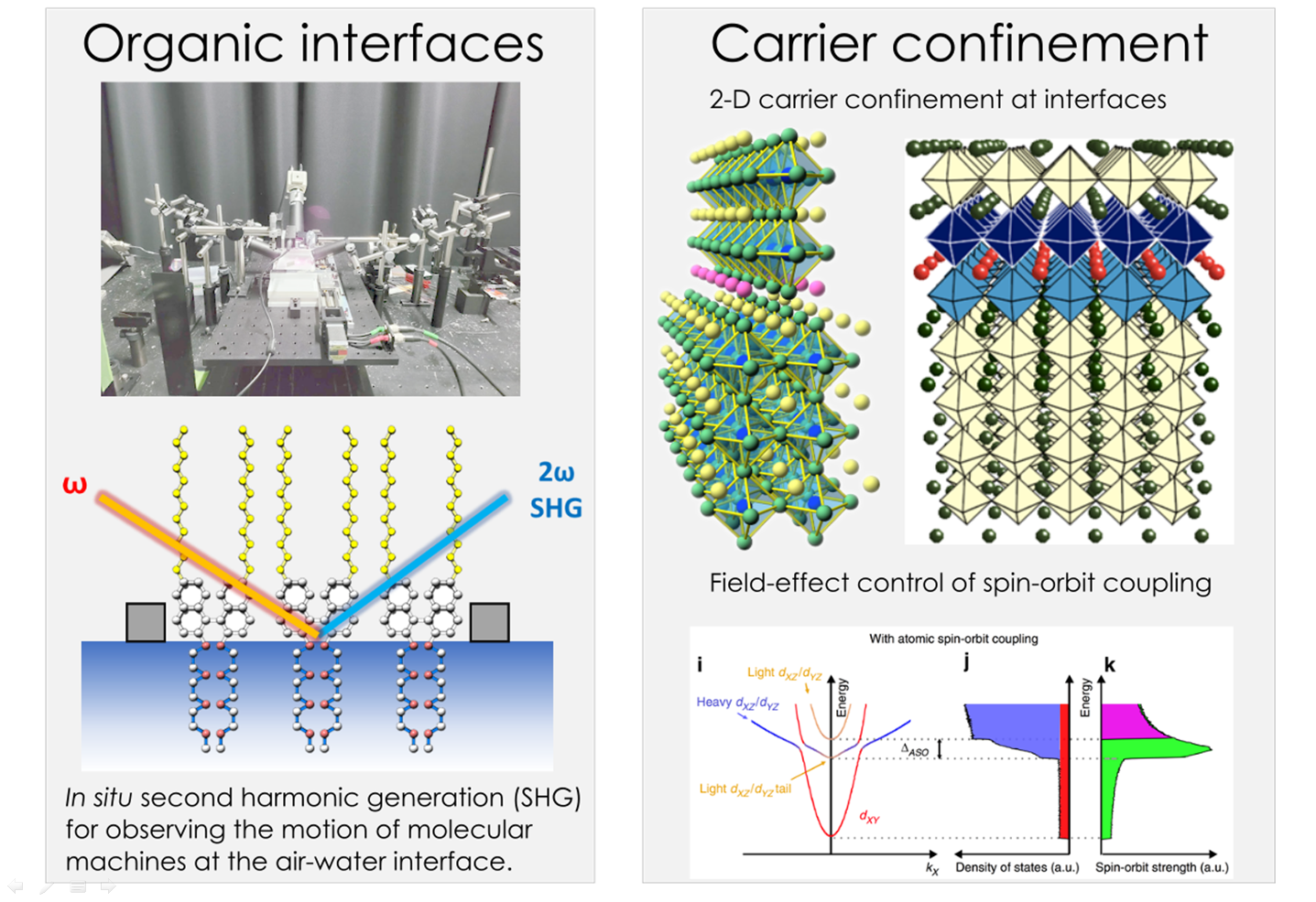
Interfaces: Just like surfaces, interfaces offer a new playground
for materials design and for quasi-two-dimensional physics. We study the
growth and behavior of various interface layers, including Ruddlesden-Popper
structures and tunnel junctions.
Techniques: We offer various projects on technique design, either
for developing crystal growth methods or developing surface analysis tools,
such as ion scattering spectroscopy.
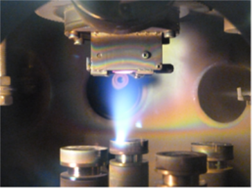
Oxide thin films
made by Pulsed Laser Deposition
Crystal is grown one atomic layer or unit cell at a time. This is a useful
technique for materials design, making nanostructures, heterostructures,
and electronic device structures, such as transistors or tunnel junctions.
Some examples of topics on offer to new students:
Ferroelectricity related to cation or charge order
Magnetoelastic interactions
Catalytic surfaces, surface nanostructures
Transport and magnetism in nanostructure arrays
Novel crystal growth techniques
Ferroelectric and multiferroic materials
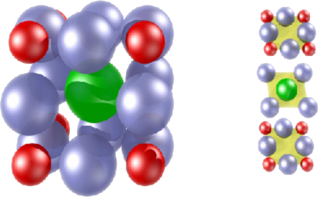
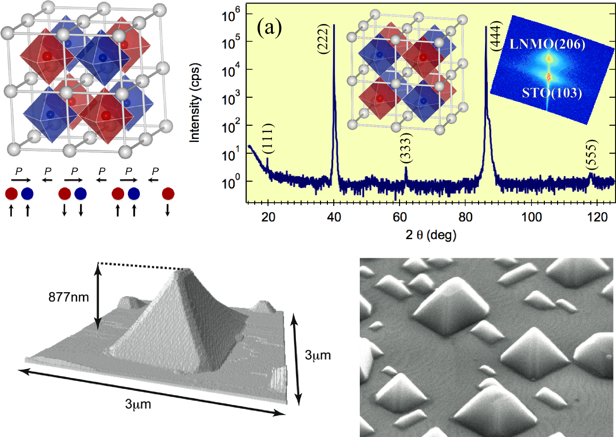
Ordered perovskite structures offer new and interesting ways of
constructing polar and ferroelectric materials. Ordering can be seen
by x-ray diffraction analysis. Ferroelectricity is related to
bond length variations.
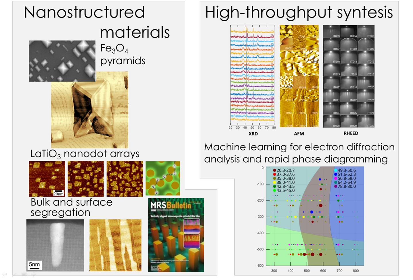
Magnetoelastic coupling is studied in nanostructured thin films, such as arrays
of magnetite nanopyramids. This project is suitable for students
interested in new materials development.
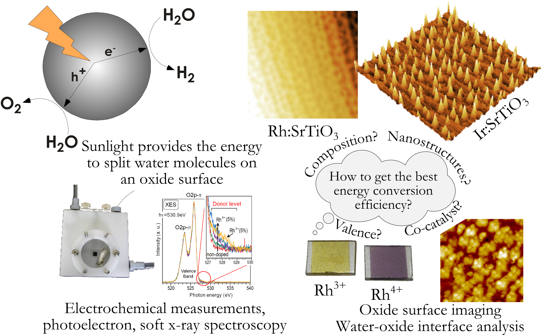
Photocatalytic materials for hydrogen production
New projects in this area are related to developing new types of heterostructures for photo-
catalysis. The work involves heterostructure growth and electrochemical characterization.
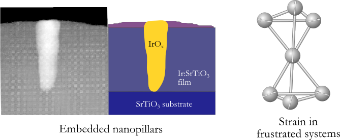
Iridate thin films and nanostructures
Platinum-group elements in oxides are less common, but offer a number of interesting
possibilities for materials design. Pt, Ir, Rh, etc. are well-known catalytic materials. We are
interested in nanostructured Ir and Pt for catalysis.
Another reson to study iridates is the strong spin-orbit coupling and interesting magnetic
states in magnetically frustrated iridate pyrochlores.
This project offers opportunities for nanostructure growth and anlaysis for students
interested in crystal design. The pyrochlore projects is more physics oriented and
fits people interested in 2D physics, surface states, and electron spectroscopy.
A new student would work with a postdoc and one PhD student.
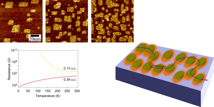
Nanostructure growth Transport in nanostructure arrays
New projects in this area are related to developing new types of heterostructures for
photocatalysis and for looking at scattering or localization mechanisms
in quai-two-dimensional systems. The work involves heterostructure growth and
transport characterization.
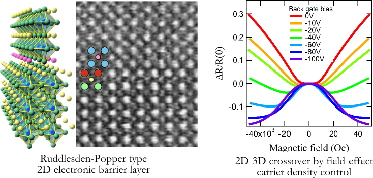
Two-dimensional electron systems at heterointerfaces
Layered oxide structures create natural barrier layers in a crystal, resulting in highly anisotropic physical properties. In this project we mostly look at transport, magnetic behavior
and carrier density control in 2-dimensional interface layers.
The project is suitable for students interested in device design on an atomic scale. It is also
possible to focus either on synthesis and measurement or on analysis of transport data.
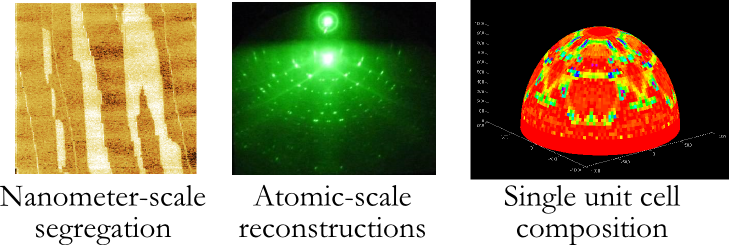
Surface analysis by AFM/STM, RHEED and CAICISS
Oxide materials can have very complicated crystal structures due to the large number of
different cations in the lattice. The surface structures are therefore often poorly known.
We offer a possibility to study the atomic-scale structure of oxide materials by various
surface analysis techniques, including STM and AFM, either x-ray or electron diffraction,
LEED analysis, and by ion scattering spectroscopy.
This project is suitable for students interested in functional materials and surface design
or for students who would like to work on surface science oriented topics.
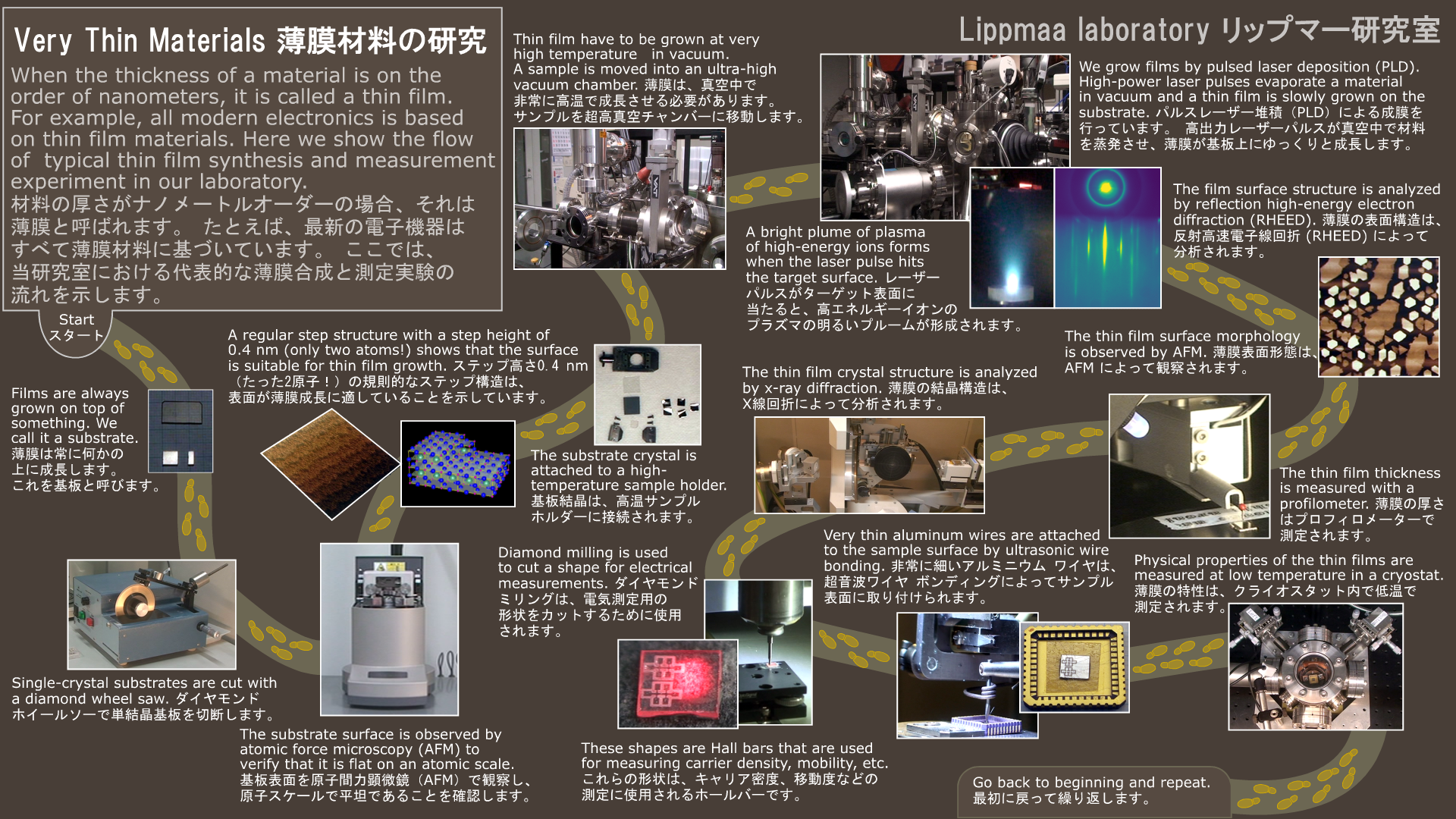
A typical work day
The ususal workflow of preparing thin film samples looks something like this:
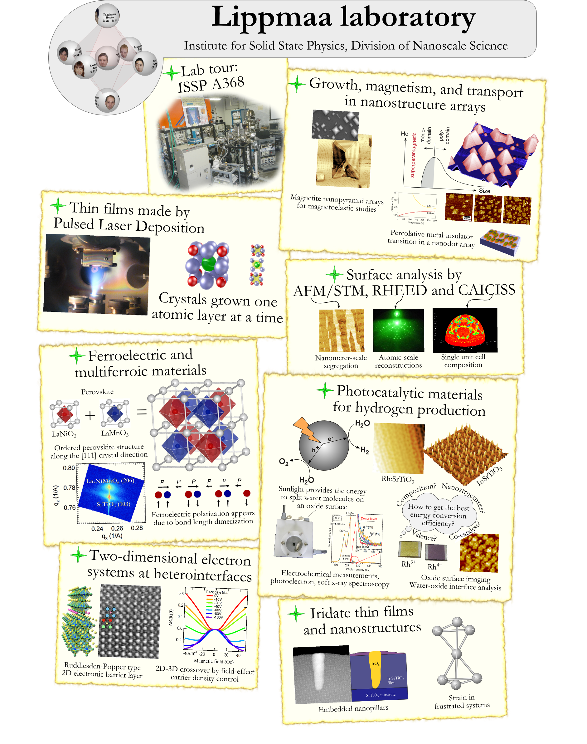
The laboratory introduction poster
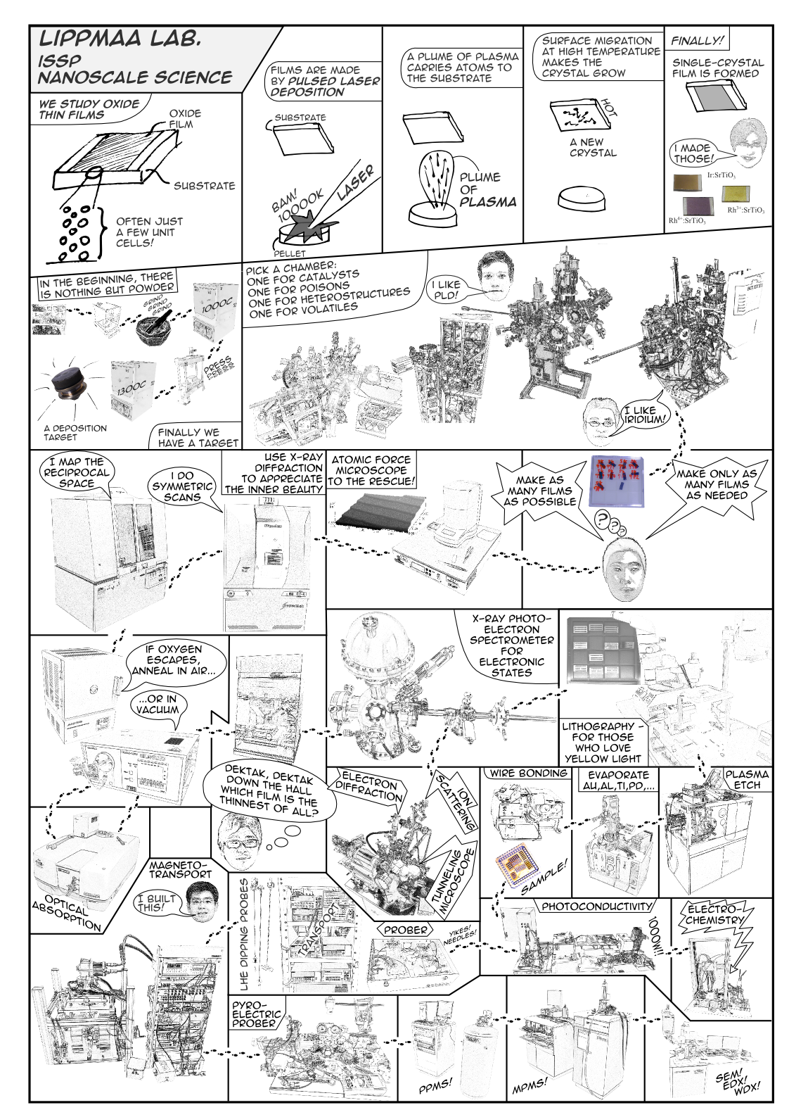
The laboratory equipment poster. Students joining the lab will have to learn
to use most of these instruments.


 Crystal is grown one atomic layer or unit cell at a time. This is a useful
technique for materials design, making nanostructures, heterostructures,
and electronic device structures, such as transistors or tunnel junctions.
Some examples of topics on offer to new students:
Crystal is grown one atomic layer or unit cell at a time. This is a useful
technique for materials design, making nanostructures, heterostructures,
and electronic device structures, such as transistors or tunnel junctions.
Some examples of topics on offer to new students:
 Ordered perovskite structures offer new and interesting ways of
constructing polar and ferroelectric materials. Ordering can be seen
by x-ray diffraction analysis. Ferroelectricity is related to
bond length variations.
Ordered perovskite structures offer new and interesting ways of
constructing polar and ferroelectric materials. Ordering can be seen
by x-ray diffraction analysis. Ferroelectricity is related to
bond length variations.